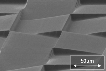
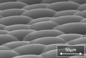
High precision processing by ultraprecision machining and lithography
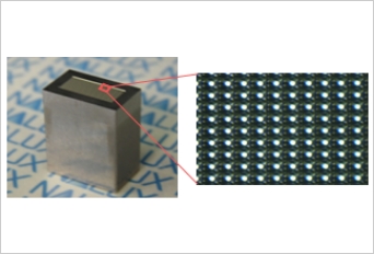
NALUX uses ultra-precision machine processing and lithography to manufacture molding tools for optical elements as well as optical elements. Ultra-precision machin processing is mainly used for refractive optics of relatively simple shapes such as rotationally symmetric aspherical surfaces and more complicated free-form optics, and lithography is mainly used to process DOE (Diffractive Optical Elements) such as gratings and CGH (Computer Generated Hologram). Lithography process is generally used to process on flat optical substrates, but NALUX provides the process which two different technologies integrated such as applying lithography on curved surface created by ultra precision processing machine.
In addition to existing state-of-the-art facilities and equipment, NALUX is constantly working on the evolution of mold processing technology, and collaborating on R&D works with processing machine manufactures. We have a number of high-precision measuring instruments to evaluate processing precision and errors. We are also developing compensation technologies to feed back evaluation results to processing works. Furthermore, in order to improve the processing environment, we have invested on our workshops and buildings to house high precision machines in order to ensure ultra precision processing excuted in appropriate manners.
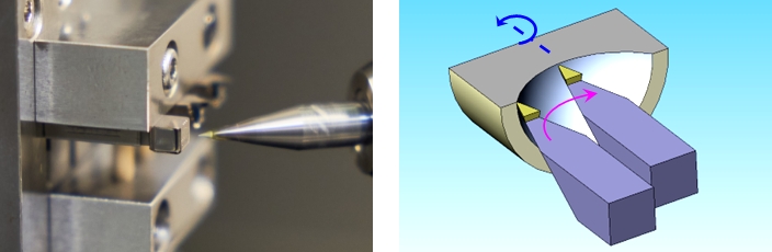
A.Ultra precision machine processing
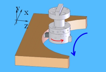
For ultra precision processing, machine tools with positioning accuracy of nano meter order is used. We have machines with 2 to 5-axes lathes, and choose appropriate one depending on the shape of the processing.
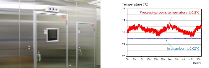
Especially in the finishing process of free form lens molds, it takes from several hours to several days. We have invested on workshop infrastructure such as high precision air-conditioning and vibration proof foundation. Because changes in workshop environment during processing give substantial impacts on product's quality.
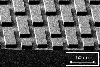
B.Lithography
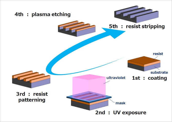
The Core technology in lithography are mainly UV mask lithography and patterning and deposition/etching by electron beam lithgraphy.
Lithography is a rapidly developing field in the semiconductor industry in recent years. A lot of attentions drawn on its miniturization processing technologies, specifically sub-10nm level line width and depth creation in semiconductor industry.
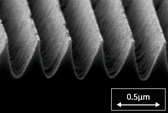
In diffractive optics mamufacturing, different expertise and experiences are required from semicoductor. Because it requires larger scale than semiconductor industry, such as 10nm to wave length order level line width and depth.
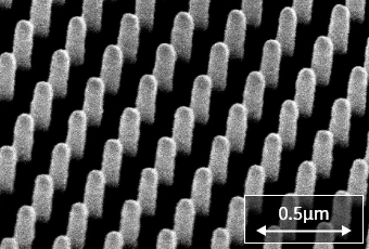
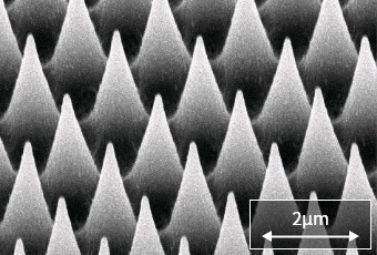
At Nalux's the Sendai Technical Research Institute, we are developing advanced lithography technology using Tohoku University's semiconductor processing equipment (i-line steppers, UV imprinting equipment, laser drawing lithography equipment, plasma CVD, plasma etching attachment, etc.). We are particularly engaged in the development of processing technologies for microlens arrays and other refractive optics by using gray scale laser lithography in addition to diffraction gratings which we have worked as targets.